Deutscher Zukunftspreis 2026
“Photonics is getting closer and closer to being applied in processors”
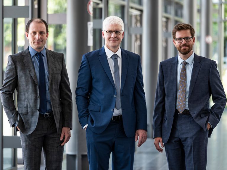
From left to right: Philipp-Immanuel Dietrich (CEO of Keystone Photonics), Christian Koos and Matthias Lauermann (Technology Fellow at Vanguard Automation). Image: Deutscher Zukunftspreis/Ansgar Pudenz
In the future, we’ll be able to use light to transmit huge amounts of data faster and more energy-efficiently. Christian Koos from the Karlsruhe Institute of Technology (KIT) is developing new methods that will make it possible to manufacture such systems even better and more efficiently. For translating his research into marketable applications, he has now been nominated for the Deutscher Zukunftspreis (German Future Prize) 2026, along with Philipp Dietrich and Matthias Lauermann.
Mr. Koos, what exactly have you and your team developed?
We work in the field of integrated photonics. The basic idea is to integrate optical components into microchips in a manner similar to electronic circuits. However, this is more difficult than in electronics. Photons have no electric charge and therefore can’t simply be guided through conductive materials. When it comes to photons, the geometry of the structures is crucial, and these structures often need to be three-dimensional.
Accordingly, our idea was to equip optical microchips – which until now have largely been two-dimensional in design – with high-precision three-dimensional structures. We can print these directly onto or between chips using femtosecond lasers. This allows light, for example, to be guided into and out of the chips more effectively. It also makes it easier to connect them and to test them during manufacturing. As such, the core of our innovation consists in making integrated photonic systems with 3D-printed structures more powerful and, at the same time, more suitable for industrial use.
Why is optical data transmission so interesting right now?
Today, we generate, transmit and process enormous amounts of data, and artificial intelligence is making demand grow even faster. As a result, especially at large data centers, massive data streams have to constantly be moved back and forth between different processors, memory blocks, and other components.
At high data transmission rates, electrical connections quickly reach their limits. Even over short distances, the signal degradation in copper cables becomes so great that the signals can no longer be detected. Light, on the other hand, can be transmitted very quickly through optical fibers with comparatively low losses. That’s why optical data transmission is getting closer and closer to being applied to actual computers – and even inside them. In the future, light signals could be transmitted not only between data centers or servers, but also between individual chips on a circuit board. Processors and memory will continue to operate electronically, but photonic components will serve as interfaces, converting electrical signals into optical ones and back again. This will accelerate signal exchange while simultaneously reducing energy consumption – and will be particularly crucial for large AI data centers, as their power consumption is already enormous and can’t continue to grow indefinitely. That’s why integrated photonics is a key means of reducing energy consumption in data transmission.

Prof. Christian Koos is a professor at Karlsruhe Institute of Technology, Institute of Photonics and Quantum Electronics (IPQ) since 2010. Image: Deutscher Zukunftspreis / Ansgar Pudenz
And are you already applying this outside your laboratories?
Yes. We’ve already launched two spin-off companies based on this research. Building on our findings, Vanguard Automation has developed machines and processes that enable optical connections and high-precision 3D structures to be fabricated directly on chips. In turn, Keystone Photonics uses the same technology to produce specialized probes that allow photonic chips to be tested while still on the wafer – the semiconductor wafer, that is. This makes it possible to identify early on which components work and which don’t, before they undergo further processing and are installed. This aspect is essential for being able to build complex systems in the first place.
These aren’t the only two spin-offs you’ve been involved with. How do you know when a scientific idea can actually become a product?
Of course, you’re enthusiastic about your own research – otherwise, you wouldn’t be doing it. That’s why you sometimes tend to overestimate its potential impact. For me, therefore, an important indicator is whether a company is willing to try out an idea and invest money in it.
If a potential customer says early on, “We’d like to launch a feasibility study and are willing to invest in it,” then I know we’ve clearly identified a real need. But that’s when the real work begins: machines, materials, processes, and software must all be combined so that the research results can be turned into a reliable and scalable technology.
And if this step is successful: Where might we see your technology five or ten years from now?
We probably won’t see it directly, since it works in the background. If the technology continues to gain traction as it’s now doing, though, it could be found in many data centers and data networks in the future. This is already partly the case today. The first photonic chips tested with our technology are already being used at AI data centers. So when we use artificial intelligence-based applications, it’s quite possible that these chips are already at work in the background.
What does the nomination for the German Future Prize mean to you personally?
The nomination is a great success for us. What unites the three of us as a team is not only our passion for research, but also our goal and our commitment to put it into practice. Of course, we don’t yet know whether we’ll ultimately win the prize. But being nominated draws attention to our work and shows that scientific ideas can be transformed into applications with very concrete economic and innovative potential. For us, this means a lot of attention and, hopefully, a boost for current and future projects.


Readers comments